Orientation

Compose a larger design from reusable blocks

Objective

Use a supplied 32-bit counter, build a 4-to-1 eight-bit multiplexer and a decoder in Verilog, generate reusable symbols, integrate the blocks in a schematic, and verify the resulting LED behaviour.

Counter

Produces many bits that toggle at progressively lower frequencies.

Multiplexer

Selects one eight-bit counter slice and routes it to the next block.

Decoder

Converts a three-bit value into an active output line.

Get the Lab 4 files.

Open the Lab 4 SharePoint folder and download the supplied project files. Extract the Lab 4 project folder, open Lab4.qpf, and work in Lab4.bdf. Lab4 is the top-level entity. Its altpll0 block divides the DE0-Nano CLOCK_50 input to CLOCK_5, which drives the simple_counter block and exposes Count[31:0].

Reuse the workflow you already know.

Opening a project, compiling, assigning pins, programming through USB-Blaster, and testing switches/LEDs follow the Lab 2 and Lab 3 workflow. This lab concentrates on counter division, multiplexing, decoding, and hierarchy.

Need a refresher?
→ FPGA Design Flow · → DE0-Nano Board Reference

Counter reasoning

Relate counter bits to observable frequencies

Quartus block diagram showing the Lab 7 counter receiving CLOCK_50 and producing Count[31:0].
Reference: the supplied counter block exposes the 32-bit Count bus used in this lab.

The supplied project first divides the board’s 50 MHz input clock by ten. The binary counter therefore advances on a 5 MHz CLOCK_5 signal. Output bit n completes a full cycle at 5,000,000 / 2n+1 hertz; every successive bit has half the frequency of the previous bit.

Human-visible behaviour

Low-order bits change too quickly for your eyes to resolve. Higher-order bits are slower; bit 23 is about 0.30 Hz, so it changes state roughly every 1.68 seconds and can be observed directly.

Counter-frequency calculations
Counter bitExpressionYour frequency (0.000 Hz)Check
225,000,000 / 223
235,000,000 / 224
295,000,000 / 230

Need a refresher?
→ Binary Counters as Frequency Dividers

Multiplexer reasoning

Choose which counter bits reach the LEDs

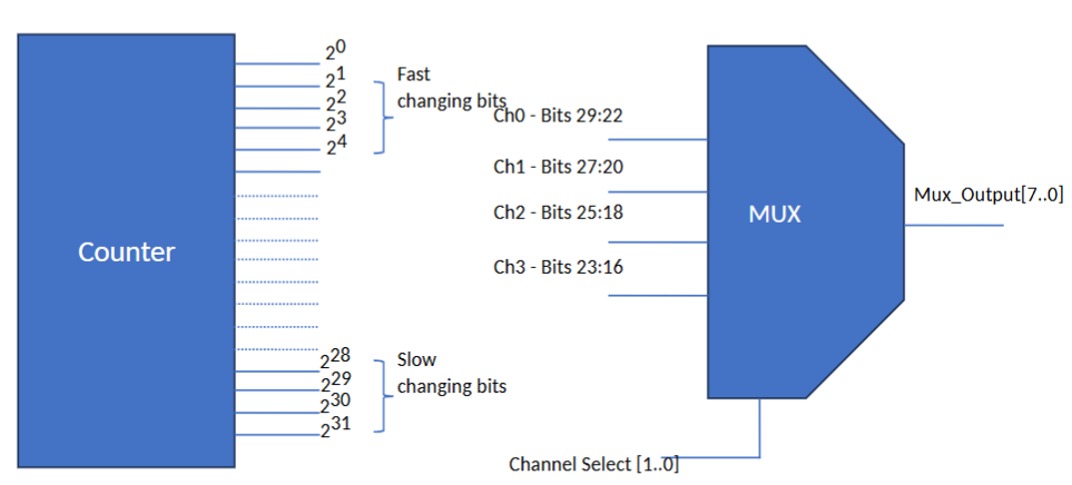
Concept diagram showing a 32-bit counter feeding four eight-bit slices into a four-channel multiplexer selected by a two-bit channel select.
The MUX picks one group of eight counter bits and sends that group to the LEDs.

The two switches labelled sel[1:0] choose the group. For each row, choose the matching input name: a, b, c, or d.

Which counter slice does each switch setting select?
Switch settingChoose this inputEight counter bits sent to the MUX outputCheck
00Count[29:22]
01Count[27:20]
10Count[25:18]
11Count[23:16]

Need a refresher?
→ Multiplexers

Supplied Verilog

Create the multiplexer module

Create a Verilog HDL file named mux_4.v. The supplied implementation uses a combinational always @(*) block and a case statement to select one eight-bit input.

Supplied code — mux_4.v
module mux_4 (
  input      [7:0] a,
  input      [7:0] b,
  input      [7:0] c,
  input      [7:0] d,
  input      [1:0] sel,
  output reg [7:0] mux_out
);
  always @(*) begin
    case (sel)
      2'b00: mux_out <= a;
      2'b01: mux_out <= b;
      2'b10: mux_out <= c;
      2'b11: mux_out <= d;
    endcase
  end
endmodule

  1. Save the file as mux_4.v and add it to the current project.
  2. Run Analysis & Synthesis and resolve errors before generating its symbol.
  3. Compare the four case items with your completed selection table.

Need a refresher?
→ Combinational Logic in Verilog

Hierarchical design

Make a block from your MUX code

Quartus can turn your mux_4.v file into a block symbol. You can then place that block in your larger schematic.

  1. Open mux_4.v.
  2. Choose File → Create/Update → Create Symbol Files for Current File.
  3. Open the main BDF and choose the new mux_4 symbol from the Project library.
  4. Check that the block has inputs a, b, c, d, and sel, plus the output mux_out. Each bus should be eight bits wide, except sel, which is two bits wide.
What you are checking: the symbol is a shortcut for your tested MUX code. It lets you connect the MUX without drawing its internal logic again.

Need a refresher?
→ Creating and Reusing Quartus Symbols

Schematic integration

Connect the counter to the multiplexer

Quartus schematic showing Count[29:22], Count[27:20], Count[25:18], and Count[23:16] connected to the four mux inputs, with speed[1:0] driving the select input and LEDs[7:0] at the output.
Reference: connect the four counter slices and the select bus to the MUX symbol as shown.

Open Lab4.bdf, the supplied top-level BDF. It already contains the altpll0 and simple_counter blocks. Place your mux_4 symbol, then make the exact bus connections below.

Counter-to-MUX connections
Counter bus sliceMUX port
Count[29:22]a[7:0]
Count[27:20]b[7:0]
Count[25:18]c[7:0]
Count[23:16]d[7:0]
sel_speed[1:0]sel[1:0]
mux_out[7:0]LEDs[7:0] for the MUX-only test

Physical assignments

Verified DE0-Nano locations
SignalLocationBoard resource
CLOCK_50PIN_R850 MHz clock
sel_speed[1]PIN_M1DIP switch 0
sel_speed[0]PIN_T8DIP switch 1
LEDs[7:0]PIN_L3, PIN_B1, PIN_F3, PIN_D1, PIN_A11, PIN_B13, PIN_A13, PIN_A15LED7 through LED0

Need a refresher?
→ Block Diagram/Schematic Files · → Using Pin Planner

Physical verification

Compile, program, and compare all MUX selections

Compile the integrated design, program the DE0-Nano, and test all four select combinations. Observe the relative LED rates long enough to distinguish the slower channels.

MUX hardware verification
sel[1:0]Expected counter sliceObserved relative LED patternMatches routing?
00Count[29:22]
01Count[27:20]
10Count[25:18]
11Count[23:16]

Decoder reasoning

Derive the active-high 3-to-8 decoder behaviour

The decoder uses mux_out[2:0] as a three-bit input. A conventional active-high 3-to-8 decoder asserts exactly one of eight outputs for each input value. Complete the table before reviewing the supplied module.

Active-high decoder table
in_count[2:0]Output that should be HIGHCheck
000
001
010
011
100
101
110
111

Need a refresher?
→ Decoders and Active Logic

Decoder implementation

Create, integrate, and verify the decoder

Quartus schematic showing a MUX feeding To_decoder[7:0] and a DecoderSimple block driving LEDs[7:0].
Reference: route the selected MUX output into the decoder, then connect the decoder outputs to the LEDs.
Implementation decision: the lab specifies a decoder and asks you to observe a one-hot LED sequence. The provided rows for 101, 110, and 111 conflict with that stated intent, so this corrected complete active-high 3-to-8 implementation is the student starting point.
Starter code — DecoderSimple.v
module DecoderSimple (in_count, decoder_out);
  input      [2:0] in_count;
  output reg [7:0] decoder_out;

  always @(*) begin
    case (in_count)
      3'b000: decoder_out = 8'b00000001;
      3'b001: decoder_out = 8'b00000010;
      3'b010: decoder_out = 8'b00000100;
      3'b011: decoder_out = 8'b00001000;
      3'b100: decoder_out = 8'b00010000;
      3'b101: decoder_out = 8'b00100000;
      3'b110: decoder_out = 8'b01000000;
      3'b111: decoder_out = 8'b10000000;
    endcase
  end
endmodule

  1. Save the decoder as DecoderSimple.v, synthesize it, and generate its symbol.
  2. Replace the direct MUX-to-LED connection: connect mux_out[2:0] to in_count[2:0].
  3. Connect decoder_out[7:0] to LEDs[7:0], compile, check assignments, and program the FPGA.
  4. Observe the one-hot LED sequence for the counter values produced at each MUX selection.

Think it through

Explain the integrated system

Completion

Prepare your Lab 4 submission package

Submission package

Download your Lab 4 submission ZIP

The ZIP includes completion.json, your MUX and decoder Verilog sources, and the integrated BDF.

Submission Details

Enter all four required details before downloading.

Generating this local ZIP does not submit work to Avenue. Evidence files must be reselected after reopening the page.