Orientation

Build a two-floor display from physical logic

Objective

Test a common-anode seven-segment display, control it with an SN74LS47 BCD decoder/driver, and design NAND/NOT logic that converts two elevator pushbuttons into the BCD inputs for floors 1 and 2.

Character test

Verify all seven segments, then form the character L.

BCD verification

Display and record decimal digits 0 through 9.

Elevator interface

Derive, build, and demonstrate two floor-button states.

Power OFF before wiring.

Remove bench power before adding, removing, or moving IC, display, resistor, pushbutton, or jumper connections. Set the supply to 5 V with a protective current limit while disconnected, and obtain the required instructor check before first power-up.

Required materials
PartQuantityRole
SN74LS471BCD-to-seven-segment decoder/driver
CD74HC05E1Six open-drain inverters
SN74LS202Four total 4-input NAND gates
INND-TS40RAB1Common-anode red seven-segment display
220 Ω resistors7One current limiter per segment
100 Ω resistors3 provided; 1 usedCommon-anode protection connection shown in the display circuits
1 kΩ pull-up resistors4Two pushbutton nodes and two used HC05 outputs
Pushbuttons4 provided; 2 usedFloor 1 and Floor 2 commands
Breadboard and jumper wires1 setPhysical construction

Component preparation

Read the package before placing the part

For every DIP IC, find the notch or dot, identify Pin 1, and count pins counter-clockwise when viewed from above. Place each IC across the breadboard centre channel. Verify the exact marking before using a pin diagram.

Verified component behavior
PartSupply and packageBehavior needed here
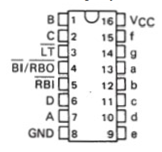
SN74LS47N16-pin PDIP; Pin 16 VCC, Pin 8 GND; 4.75–5.25 VBCD A–D inputs; active-LOW open-collector segment outputs a–g; LT, RBI, and BI/RBO controls
CD74HC05E14-pin PDIP; Pin 14 VCC, Pin 7 GND; operate at 5 V hereSix inverters with open-drain outputs. Every used output requires a pull-up; unused inputs must be tied to a defined level.
SN74LS20N14-pin PDIP; Pin 14 VCC, Pin 7 GND; 4.75–5.25 VTwo independent 4-input positive-NAND gates. Every input of a used gate must be defined.
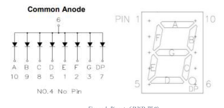
INND-TS40RAB10-lead through-hole display; common anode at Pin 6; Pin 4 has no connectionSegment pins: a=10, b=9, c=8, d=5, e=1, f=2, g=3, decimal point=7
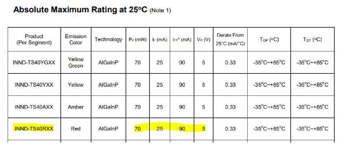
SN74LS47 display-driver datasheet table highlighting the INND-TS40RXX red display row and its 70 mW power rating, 25 mA current, and 5 V rating
Datasheet reference for the red INND-TS40 display ratings. Treat these as limits, not target operating values.
Common-anode INND-TS40 display diagram identifying segments a through g, decimal point, common-anode Pin 6, segment pin numbers, and unused Pin 4
Seven-segment display segment naming and pin identification
Top-view SN74LS47 16-pin package pinout showing B, C, lamp test, blanking controls, D, A, ground, segment outputs e through f, and VCC
SN74LS47 top-view pin identification
Interface constraint

A 74LS output HIGH is not guaranteed to reach the 3.15 V HIGH threshold of a 5 V HC input. Do not route an SN74LS20 output directly into a CD74HC05E input. A pulled-up HC05 output can feed an LS20 input.

Need a refresher?
→ Reading Digital-IC Datasheets · → TTL and CMOS Logic Families

Display subsystem

Test every segment before adding logic

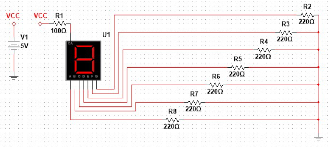
Five-volt common-anode seven-segment test circuit with common anode connected through 100 ohms to 5 volts and seven separate 220 ohm segment resistors connected to ground
Seven-segment display test circuit
  1. Power off: place the display and confirm its orientation. Connect common-anode Pin 6 to +5 V through the 100 Ω protection resistor shown.
  2. Connect each segment pin a–g through its own 220 Ω resistor to ground. Leave decimal-point Pin 7 disconnected.
  3. Ask the instructor/TA to inspect the display orientation, resistor placement, +5 V rail, and ground rail. Record the check below before applying power.
  4. Apply the current-limited 5 V supply. Confirm that all seven segments illuminate.
  5. With power off between changes, disconnect the segment resistors that are not needed to form the character L. Reapply power and observe the result.
Why LOW turns a segment on

The display’s segment anodes share +5 V. Current flows only when a segment cathode has a path toward ground. Grounding that cathode through its resistor therefore illuminates the segment.

Need a refresher?
→ Seven-Segment Displays

Decoder subsystem

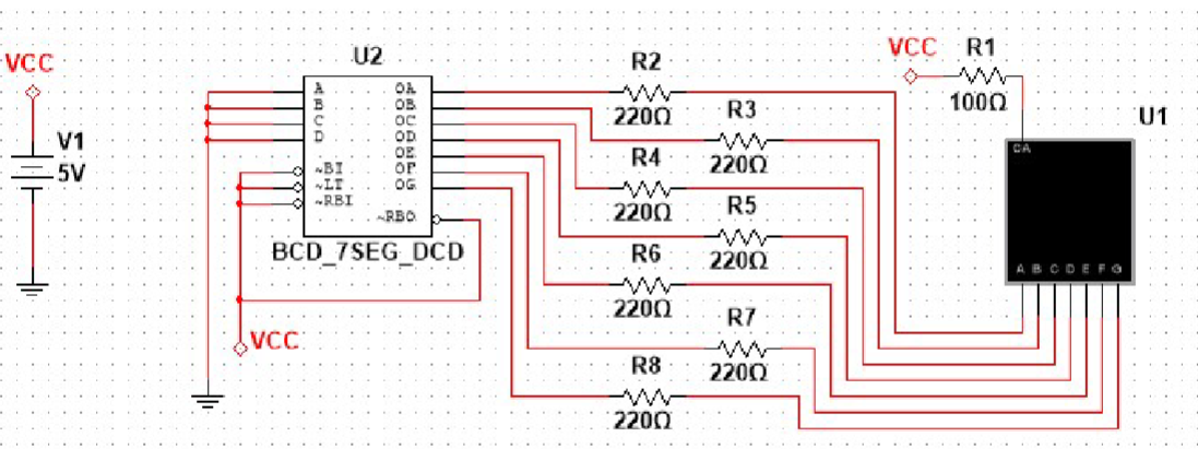
Wire the SN74LS47 to the common-anode display

Five-volt SN74LS47 BCD decoder connected through seven individual 220 ohm resistors to a common-anode seven-segment display
BCD decoder/driver and common-anode display circuit
  1. Power off: insert the SN74LS47 across the centre channel. Connect Pin 16 to +5 V and Pin 8 to ground.
  2. For normal display operation, hold LT (Pin 3), BI/RBO (Pin 4), and RBI (Pin 5) HIGH at +5 V. Do not leave control inputs floating.
  3. Connect outputs a–g to the matching display segment pins through seven separate 220 Ω resistors: a Pin 13, b Pin 12, c Pin 11, d Pin 10, e Pin 9, f Pin 15, g Pin 14.
  4. Connect display common-anode Pin 6 to +5 V. Keep the decimal point disconnected.
  5. Initially connect B (Pin 1), C (Pin 2), D (Pin 6), and A (Pin 7) to ground for BCD 0000.
  6. Obtain an instructor/TA wiring check, apply the current-limited 5 V supply, and confirm digit 0.
Current path: +5 V enters the common anode, passes through an illuminated LED segment and its 220 Ω resistor, then enters an active-LOW SN74LS47 open-collector output that sinks current to ground.

Need a refresher?
→ BCD-to-Seven-Segment Decoder/Drivers · → Open-Collector and Open-Drain Outputs

BCD verification

Display decimal digits 0 through 9

Work one row at a time. Turn the power off before changing wires. Set the four inputs D, C, B, and A, then type those four switch values in the second column. Turn the power on, look at the seven-segment display, and type the digit you see in the third column.

How to use this chart:

The number on the left is the digit you are testing. In the second column, type the four switch values you used, in the order D C B A. In the third column, type the digit that actually appears on the display. The last column reports whether both entries are correct.

Enter your switch settings and the digit you see
Digit to testYour D C B A settingsDigit shown on displayCheck
0
1
2
3
4
5
6
7
8
9

Scope: codes 1010 through 1111 are not valid single-digit BCD. Do not depend on a particular displayed result for those codes in this experiment.

Upload three display photos:

Take one clear photo while the display shows 0, one while it shows 5, and one while it shows 9. Each photo should show the lit digit and enough of the decoder/display wiring to identify the circuit. Select the three image files below; they are added to the local ZIP and are not submitted to Avenue automatically.

Need a refresher?
→ Binary-Coded Decimal

Input subsystem

Build and test two active-LOW pushbuttons

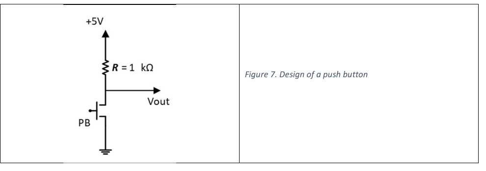
Pushbutton input circuit with a 1 kilohm pull-up resistor from 5 volts to Vout and a normally-open pushbutton from Vout to ground
Defined pushbutton input using a 1 kΩ pull-up
  1. Power off: build two copies, labelled Floor 1 and Floor 2. Each output node connects through 1 kΩ to +5 V and through its pushbutton to ground.
  2. Check pushbutton terminal pairs with continuity while power is off; four-pin tactile switches often connect same-side pins internally.
  3. Apply 5 V and measure each output relative to circuit ground when released and pressed.
  4. Remove power before connecting these outputs to IC inputs.
What to record:

Measure the button output voltage with your multimeter. Record one reading while both buttons are released, then record one reading while the button you are testing is pressed. “Released” means no button is being pressed. “Pressed” means the selected button is held down. Keep the black meter lead connected to circuit ground.

Logic design

Derive the two-floor encoder

Design combinational logic that produces BCD 0001 when only Floor 1 is pressed and BCD 0010 when only Floor 2 is pressed. Connect BCD_C and BCD_D permanently to ground. Treat neither-button and both-button states as invalid commands: your design must produce a defined output, and you must document the chosen behavior.

Elevator logic requirements
Floor 1 buttonFloor 2 buttonMeaningRequired/defined BCD output
ReleasedReleasedNo request
PressedReleasedFloor 10001
ReleasedPressedFloor 20010
PressedPressedConflicting request
Implementation constraints
  • Use the available CD74HC05E NOT gates and SN74LS20 4-input NAND gates.
  • Add a 1 kΩ pull-up from +5 V to every used HC05 open-drain output.
  • Do not drive an HC05 input from an LS20 output. Arrange the design so HC05 outputs feed LS20 inputs; use a NAND gate with all inputs joined when an LS-family inversion is needed.
  • Tie unused HC05 inputs to ground. Tie every unused input of each used SN74LS20 gate to a defined HIGH or LOW as required by your expression.

Need refreshers?
→ Boolean Simplification · → Basic Logic Gates

Physical integration

Build the NAND/NOT logic and connect the decoder

  1. Power off: place one CD74HC05E and both SN74LS20 ICs across the centre channel with aligned notch orientation.
  2. Connect Pin 14 of each 14-pin IC to +5 V and Pin 7 to ground. Keep the SN74LS47 at the same +5 V/common-ground rails.
  3. Wire your reviewed logic schematic using verified gate pinouts. Install each required open-drain pull-up before connecting the next stage.
  4. Connect the logic outputs to SN74LS47 BCD_A (Pin 7) and BCD_B (Pin 1). Tie BCD_C (Pin 2) and BCD_D (Pin 6) to ground.
  5. Audit every IC input: each must trace to +5 V, ground, a pull-up-defined button node, or a driven logic output. No input may float.
  6. Ask the instructor/TA to inspect orientation, rails, pull-ups, family direction, decoder controls, segment resistors, and the complete point-to-point schematic comparison before power-up.
Final power audit
Device+5 VGroundOther required defined nodes
SN74LS47Pin 16Pin 8LT, BI/RBO, RBI HIGH; A–D defined
CD74HC05EPin 14Pin 7Used outputs pulled up; unused inputs grounded
Each SN74LS20Pin 14Pin 7Every gate input defined
INND-TS40RABCommon anode Pin 6Through active segment pathsOne 220 Ω resistor per segment

System verification

Test every elevator-button state

Apply the current-limited 5 V supply and test systematically. Record logic voltages with respect to circuit ground and the actual displayed result. Do not change wiring while powered.

Elevator floor-display verification
Floor 1Floor 2BCD_B (V)BCD_A (V)Observed displayMatches design?
ReleasedReleased
PressedReleased
ReleasedPressed
PressedPressed

Think it through

Explain the completed circuit

Completion

Prepare the Lab 5 submission

Keep the submission actions distinct

This page stores responses locally and packages selected evidence into a local ZIP. It does not submit to Avenue to Learn. Prepare the required single document/PDF containing your individual pictures and answers, then follow your instructor’s current Avenue submission direction.

Submission package

Download your Lab 5 submission ZIP

The ZIP includes completion.json, BCD display evidence, your logic schematic, and the completed-circuit evidence selected in this browser session.

Submission Details

Enter all four required details before downloading.

Evidence files must be reselected after reopening the page. Generating this ZIP does not submit it to Avenue.