Orientation

Make fast digital state visible

Objective

Route the 50 MHz oscillator to an LED, divide it with a binary counter and reusable module, implement frequency division with positive-edge-triggered D flip-flops, build a two-bit asynchronous counter, and compare LED brightness produced by unequal duty cycles.

Start by creating the Quartus project:

Before building any circuit, open Quartus Prime and create a new project in a local folder named wave. Set both the project name and the top-level entity name to wave. You will later create the Verilog file wave.v inside this project. Use the Cyclone IV E device EP4CE22F17C6 for the DE0-Nano.

Required resources
Resource Requirement
DE0-Nano One board and USB-Blaster connection
Quartus Prime 25.1 Lite Edition with Cyclone IV device support
Reference DE0-Nano User Manual
Board care

Disconnect board power before changing external hardware. This experiment uses only onboard LEDs and needs no power interface. Confirm the target device and pin assignments before programming.

Need a refresher?
→ Combinational vs Sequential Logic
Direct clock

Route 50 MHz directly to LED0

Create a new verilog file named wave.v and add it to the project.

DE0-Nano pin assignments used in this lab
PortLocation
CLK_50MHzPIN_R8
LED0PIN_A15
LED1PIN_A13
LED2PIN_B13
LED3PIN_A11
LED4PIN_D1
LED5PIN_F3
LED6PIN_B1
LED7PIN_L3
Starter code — wave.v
module wave(CLK_50MHz, LED0);
    input  CLK_50MHz;
    output LED0;

    assign LED0 = CLK_50MHz;
endmodule

  1. Run Analysis & Synthesis and inspect Tools > Netlist Viewers > RTL Viewer.
  2. Assign the clock and LED0 pins, compile, and program output_files/wave.sof through USB-Blaster in JTAG mode.
  3. Observe LED0. A 50 MHz signal changes too quickly for the eye to resolve as blinking; record its apparent state and explain it.

Need refreshers?
→ Clock Signals and Active Edges · → RTL Viewer and Technology Mapping

Counter divider

Expose binary-counter frequencies

Counter divider — wave.v
module wave(CLK_50MHz, LED0, LED1, LED2, LED3, LED4, LED5, LED6, LED7);
    // Declare the 50 MHz input and the eight LED outputs.
    input CLK_50MHz;
    output LED0, LED1, LED2, LED3, LED4, LED5, LED6, LED7;

    // Logic to code: make a register wide enough to hold the counter bits
    // used below. Start at zero so the design has a known first state.
    reg [26:0] count = 27'd0;

    // Logic to code: on every rising edge of the 50 MHz clock, increase the
    // counter by one. Use a nonblocking assignment for this clocked register.
    always @(posedge CLK_50MHz)
        count <= count + 1'b1;

    // Logic to code: connect selected counter bits to the LEDs. Each bit
    // toggles at a different divided frequency: f[n] = 50 MHz / 2^(n+1).
    assign LED0 = count[0];
    assign LED1 = count[1];
    assign LED2 = count[17];
    assign LED3 = count[18];
    assign LED4 = count[19];
    assign LED5 = count[20];
    assign LED6 = count[21];
    assign LED7 = count[26];
endmodule

What you must do:
  1. Copy the counter-divider code above into wave.v, replacing the direct-clock version.
  2. Compile the same wave project and program the new wave.sof to the DE0-Nano.
  3. For every row, calculate the LED frequency using f[n] = 50,000,000 / 2^(n+1), and enter your answer in the calculated-frequency box.
  4. Look at the physical board and describe what each LED does in the observation box (for example, “steady”, “too fast to see”, or “visible blink”).

The bit number in the table tells you which count bit drives that LED. You are recording both a calculation and a real-board observation; the two columns are not asking for the same thing.

Calculated and observed divider outputs
LED Bit Calculated frequency (Hz) Physical observation
LED0 0
LED1 1
LED2 17
LED3 18
LED4 19
LED5 20
LED6 21
LED7 26

Need a refresher?
→ Binary Counters as Frequency Dividers

Module divider

Package the divider as a reusable module

Adjust_Clk module and instance
// Reusable clock-divider module.
module Adjust_Clk(CLK_in, CLK_out);
    input CLK_in;
    output CLK_out;

    // Logic to code: count rising edges of the input clock in a register.
    reg [26:0] count = 27'd0;
    always @(posedge CLK_in)
        count <= count + 1'b1;

    // Logic to code: expose one slower counter bit as the module output.
    assign CLK_out = count[26];
endmodule

// Top-level module for the DE0-Nano.
module wave(CLK_50MHz, LED0, LED1);
    input CLK_50MHz;
    output LED0, LED1;
    wire CLK_low_freq;

    // Logic to code: instantiate Adjust_Clk and connect its ports in order:
    // input clock first, divided-clock output second.
    Adjust_Clk clk1(CLK_50MHz, CLK_low_freq);

    // Logic to code: show the original clock on LED0 and divided clock on LED1.
    assign LED0 = CLK_50MHz;
    assign LED1 = CLK_low_freq;
endmodule

What you must do:
  1. Replace the Counter Divider code in wave.v with the two-module code above. Keep both Adjust_Clk and the top-level wave module in the same file.
  2. Compile the same Quartus project and program the new wave.sof to the DE0-Nano.
  3. Confirm that LED0 shows the fast 50 MHz clock and LED1 shows the slower clock produced by Adjust_Clk.
  4. Measure the time for ten complete ON events of LED1. Enter that time in seconds, then use it to estimate LED1’s frequency with frequency = 10 / measured time.
  5. In the final box, explain whether your measured frequency is close to the calculated frequency for count[26].

The instance clk1 is the connection between the top-level design and the reusable divider. Do not create a second Quartus project.

Save this code before continuing:

Copy the completed two-module design into Notepad and save it as adjust-clk-stage.txt. You will copy the Adjust_Clk module from this backup into the Two-bit Counter stage after wave.v is replaced.

D flip-flop divider

Toggle a D flip-flop on each positive edge

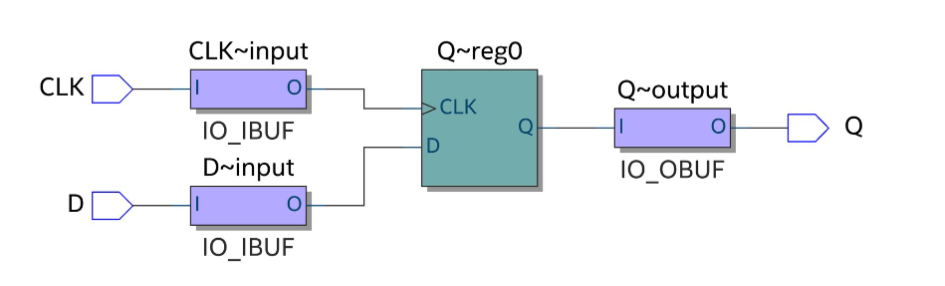
RTL viewer diagram showing clock and D inputs entering a D flip-flop and Q leaving as the output
RTL view of a D flip-flop: the stored Q output changes when the clock edge captures D.

A positive-edge-triggered D flip-flop stores D at Q only when its clock rises. Feeding Q_ back to D makes Q toggle once per rising edge and divide clock frequency by two.

D flip-flop module
// Reusable positive-edge-triggered D flip-flop.
module D_FF(D, C, Q, Q_);
    input D, C;
    output Q, Q_;

    // Logic to code: initialise Q, then store D only when C rises.
    reg Q = 1'b0;
    always @(posedge C)
        Q <= D;

    // Logic to code: make the complementary output the inverse of Q.
    assign Q_ = ~Q;
endmodule

What you must do:
  1. Replace the Module Divider code in wave.v with the D flip-flop module above.
  2. Compile the same Quartus project. You are practising the flip-flop module and its timing relationship; keep the module name D_FF.
  3. Use the supplied clock-frequency value to calculate the expected Q frequency. Enter your numeric answer in the first box.
  4. In the explanation box, describe why feeding Q_ back to D makes Q change state once per clock edge and therefore divide the frequency by two.

Need a refresher?
→ D Flip-Flops

Two-bit counter

Cascade two D flip-flop dividers

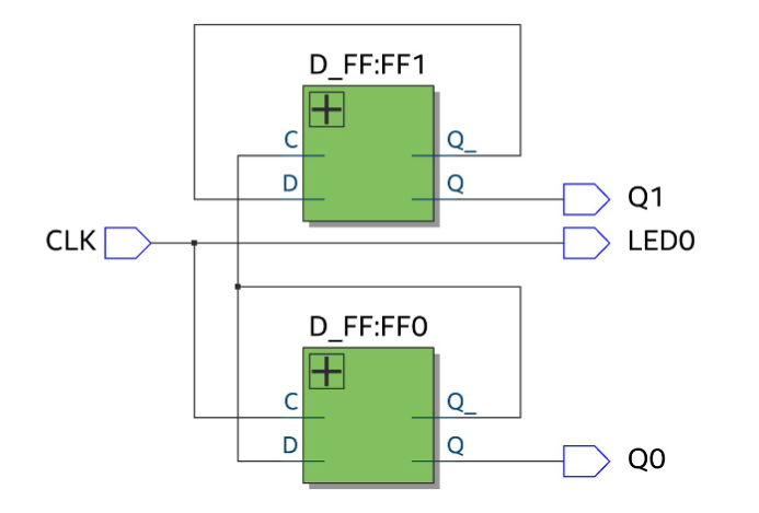
Block diagram showing two cascaded D flip-flops with feedback from each complementary output, producing Q0 and Q1
Two-bit ripple-counter connection: each D input receives its own complementary Q output.

Use the divided clock from Adjust_Clk for the first toggle stage and clock the second stage from the first stage’s complemented output. This is an asynchronous (ripple) counter: the second state transition follows the first stage rather than the original clock directly.

Build requirement: instantiate D_FF FF0 and D_FF FF1; connect each D to its own Q_; route the low-frequency clock to LED0, Q0 to LED1, and Q1 to LED2.

Need a refresher?
→ Asynchronous / Ripple Counters

Reuse your saved divider:

Open adjust-clk-stage.txt and copy the complete Adjust_Clk module into wave.v before adding the two D flip-flop instances. This preserves the divider you completed in the previous stage.

Asymmetric waveform

Predict brightness from duty cycle

Build six toggle stages. LED0 is held HIGH. LED1 through LED5 are driven by AND functions containing two through six successive counter states, producing ideal duty cycles of 1/4 through 1/64. The eye averages transitions occurring far faster than visible blinking and perceives lower average brightness.

Duty-cycle prediction
Output Expression Duty cycle (%)
LED0 1'b1
LED1 Q0 & Q1
LED2 Q0 & Q1 & Q2
LED3 Q0 & Q1 & Q2 & Q3
LED4 five-state AND
LED5 six-state AND

Need refreshers?
→ Reading Digital Timing Diagrams · → PWM & Duty Cycle

Physical verification

Compile, program, and compare brightness

  1. Complete the six-stage design using the verified D_FF module and defined internal wires.
  2. Run Analysis & Synthesis. Inspect the RTL Viewer to confirm six storage stages and the intended AND paths.
  3. Compile, confirm the assigned ports, program wave.sof, and observe LED0–LED5.
  4. Demonstrate the working clock-divider, two-bit counter, and brightness behavior to the instructor.

Analyze

Think it through

Completion

Prepare your Lab 6 submission package

Assessment distinction

Complete and export this HTML record, select files for the local ZIP, demonstrate the FPGA results and answers to your instructor, and retain the board snapshots required to support those answers. Creating the ZIP is not an instructor demonstration or an Avenue submission.

Submission package

Download your Lab 6 submission ZIP

The ZIP includes completion.json, final wave.v, RTL evidence, the waveform drawing, and FPGA-result evidence.

Submission Details

Enter all four required details before downloading.

Generating this local ZIP does not submit work. Evidence files must be reselected after reopening the page.